Description
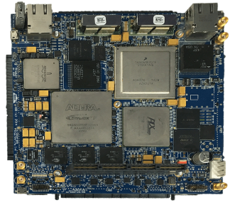
[vc_row][vc_column][vc_video link=”https://youtu.be/zVyHWGZ7AE4″ css=”.vc_custom_1550265132705{margin-top: -30px !important;}”][vc_column_text]From data ingestion to model & simulation to radar processing to computational finance to cyber security to edge analytics, the dual Stratix 10 eXtreme High Performance Compute Node, a.k.a WARP II, is the most versatile and highest performing FPGA accelerator card to hit the market!
Warp II is designed to take on today’s data-intensive computing problems by incorporating two of Intel’s revolutionary Stratix 10 FPGAs, massive amounts of DDR4 and plenty of high speed I/O. With the OpenCL support included in the Board Support Package (BSP), Warp II can be easily programmed without the need to dive down into complicated Verilog or VHDL code.
COTS, Custom Heat Sinks and Custom Solutions Available!
Are you looking for custom hardware, software, sensor or mechanical design support? Colorado Engineering Inc. (CEI) has been developing world class technology since 1990. We are proud to be a platinum member of Intel’s Design Solutions Network. Please contact us to find out how we can help you be successful with your next design project![/vc_column_text][/vc_column][/vc_row][vc_row][vc_column width=”1/2″][vc_column_text]
Features
- Dual Intel Stratix 10 FPGAs
- Up to 576 GB DDR4 (288 GB per FPGA)
- 20 TFLOPs (10 TFLOPs/FPGA)
- PCIe x16 Gen 3
- 2x QSFP + 40/100 GbE
- L tile: 40 GbE operating at 10 Gbps backplane performance
- H tile: 100 GbE operating at 28 Gbps backplane performance
- Intel Max10 FPGA
- Freescale K61 microcontroller
- GPU-sized PCIe form factor
- 4x QSFP port availability
Applications
- Communications
- Computing
- Military
- Broadcast
- Medical
- Test and measurement
[/vc_column_text][/vc_column][vc_column width=”1/2″][vc_column_text]
Specifications
Stratix 10 FPGA
GX28OUF50
-
- 96 XCVR
- 1160 user I/O
- 2.8 M logic elements
- 11,520 18×19 multipliers
- 128 GB/s FPGA-to-FPGA
- Memory bandwidth: 19.2 x 8 = 153.6 GB/s
SX FPGA (HPS): GS280UF50
-
-
- Quad ARM A53 at up to 1.2 GHz
- 4 GB DDR4-2400
- 32 KB L1 Cache
- 1MB L2 Cache
- High bandwidth FPGA bridges
- 10/100/1000 Ethernet
- USB 2.0 (On-the-Go)
- Micro SD card slot
- UART
-
DDR4 RAM**
- 8 GB discrete per FPGA
- 4x RDIMM – 256 GB Max (128 GB/FPGA*)
- 2400 MT/s
- 19.2 GB/s
I/O
- 40/100 GbE QSFP+ (25 Gbps x4)
- mUSB – B
- High speed cable connector (optional)-2×4 SerDes (16 Gbps x4)
Power/Monitor/Protect/Config
- Freescale K61 mController
- Intel Max10 FPGA
- 1024 Mb boot flash per FPGA
*May violate PCI Express full-height card
** 4 GB per FPGA is Hard Processor System (HPS)-only[/vc_column_text][/vc_column][/vc_row][vc_row][vc_column][vc_column_text]